Thursday 30 March 2023

6502 : BEN2 : Build

Once I was happy with the design and layout of my new 6502 "Ben Eater" board it was time to build and test it.

Tools

An advantage of soldering a board is that I am unlikely to suffer from bad connection problems.  The downside is that soldering errors are harder to correct.  It makes sense to build the board in small stages, regularly checking functionality as the build progresses.  My soldering ability isn't great and I felt it would be good to change my "make do" tools for better ones.  I purchased: a soldering iron with a finer tip and more / adjustable power; wire strippers and cutters suggested by Ben Eater and a circular LED craft light to provide clearer more even illumination of the workpiece.  I also purchased an SMD tester, not because I ever expect to solder SMDs but it is extremely useful as a circuit tester.  Using the SMD tester I can quickly check that there are no shorts between adjacent tracks on the strip board - a common source of problems.


Solder memory

The first component to solder was the ZIF ROM holder and adjacent header pins.  I attached the mega to the header pins on the side of the ROM holder and provided a sketch which read in the first 512 bytes of ROM data and displayed it.

Next I soldered the RAM holder and headers.  Since ROM and RAM have the same pin out I could insert my ROM chip in the RAM holder, attach the mega to the RAM header and run the same sketch to test the RAM soldering.

Next I added the wires connecting ROM and RAM holders.  The address (15) and data (8) pins on ROM and RAM are connected to each other forming busses.  This meant that I could attach the mega to the RAM header pins, which is is long-term position and put the ROM in its holder.  The remaining 5 pins (5V, GND, /WE, /OE and /CE) were then plugged into the mega at 5V or GND and my test mega sketch was able to read ROM data on the adjacent chip holder.

Step 4 was to add power connections.  There are approximate rails down the middle of the board with some posts attached for external offoard power inputs and outputs.  Power connections to chips on the board were connected to these rails or other components in a pragmatic way.  I completed all power connects for the board at this time.  I also added some clock signals and posts.

ROM testing

The final set of connections on the top row are for the NAND chip which provides control signals for ROM and RAM.  I amended my ROM test sketch to provide the NAND inputs which are made available on the extended RAM header and control the ROM.  Unfortunately the sketch did not work and I spent a long time searching for a solution to the problem.  I became extremely agitated and took a break over Christmas and through January before trying again in mid-February.  At last I found that the pinouts for the NAND chip I am using (4011CD) are slightly different from the 74HC00 in Bens circuit.  This meant that I was wiring together outputs from two NAND gates, giving indeterminate results.  Once I had diagnosed the problem it was easy to rectify my solder connections and I successfully tested reading and writing the ROM.

RAM testing

The last component which needed testing in the top half of the circuit was the RAM memory.  I wrote a sketch to test the RAM but again, unfortunately it didnt work.  To make sure I was trying to read/write RAM correctly I setup a RAM chip on breadboard and tested a standalone sketch.

When the sketch still didn't work I realised I had a duff RAM chip.  I swapped it out and my standalone test sketch worked fine.  About three out of ten of my RAM chips have been fault and a couple of others had bad pins.  They were very cheap and I reckon they may be second-hand, removed from an old board.  With a working RAM chip I was easily able to adapt my standalone sketch to work on the BEN2 board and I now have sketches which can easily test ROM, RAM and NAND.

The top half of the board comprising ROM, RAM and their NAND control logic is in working order at long last and I can start soldering connections to the bottom half of the board.  It has taken vastly longer than anticipated but I hope that the solution will be more reliable than previous attempts.

CPU

CPU memory control lines have previously been soldered.  The next step is to solder address and data bus wires to the CPU.  The board is beginning to be quite crowded / full but it isn't too tricky to access the wires.  The diagram below shows ROM+RAM+Power connections in blue and the extra connections for address and data bus in yellow.


Prior to finishing off the VIA wires I set up the CPU for testing.  I inserted a 65C02 CPU and connected the Mega, including two extra GPIO pins to monitor the clock and Reset buttons.  I connected the Ben Eater Clock board to the CPU clock.

Previously we have been concerned with testing ROM and RAM which was done rather differently from Ben Eaters original tutorials.  We had extra testing sketches to diagnose / check that memory was working.  Now we are more aligned with Ben's "Hello World" tutorial and I use the monitor sketch (adjusted for GPIO pins I am using) to check CPU initialisation.

When the Reset button is pressed the 65C02 spends 6 clock cycles then loads a reset vector from addresses $FFFC-$FFFD.  It then starts loading and executing instructions from the address specified in the reset vector.  In the test ROM I am using the reset vector is set to $8000.  Starting the 65C02 this is what we see on the monitor:  


A simplified view of memory is:

$8000 08
$8001 ff
$8002 9a
$8003 a9
......
$FFFC 00
$FFFD 80

This demonstrates that the CPU is connected to address and data busses and its initialisation sequence works.

VIA

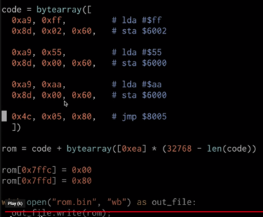
Finally we need to have a peripheral so that we can SEE our 6502 is able to DO something.  I soldered the final board wires It is traditional to use an LED for this purpose.  I referred back to Ben's tutorial video 2 which demonstrates a simple 6502 machine code program which uses VIA output pins to flash an LED.  The program only comprises 18 bytes of code so it was simple to modify my write-byte sketch to write 18 bytes.

I then connected an LED to a VIA output port.  I was thrilled that the LED went on and off as I single-stepped through the program๐Ÿ˜Š๐Ÿ˜Š๐Ÿ˜Š  This validates that the VIA is working and my board is now complete.

Conclusion

The flashing light is a suitable finale for the time spent building this hardware board.  Until the board does something you can see it is just some chips and wires.  A blinking LED is a traditional electronics "Hello World" objective with the associated satisfaction in demonstrating some mastery of the hardware/subject.

In retrospect it has been much more difficult than I anticipated to design and consturct my own layout for a Ben Eater board.  When following the Ben Eater tutorials in February 2021 I reached the end of video 2 within a week and successfully flashed my light.  However I feel I have achieved something of my own and I hope I will be able to progress smoothly through the next stages of the project.

Schematic, Layout and Board


Monday 13 March 2023

VisionFive 2 : A real computer

Purchase

Low cost RISC-V boards continue to be released with improved capabilities.  The story so far:
Allwinner Nezha 22nd June 2021
Sipeed Lichee RV 16th December 2021
MangoPi MQ-Pro 10th August 2022
Sipeed M1S 22nd December 2022
StarFive VisionFive2 delivered 7th February 2023

The latest offering, VisionFive 2 (VF2) was announced on kickstater and I subscribed on 25AUG22.


The RISC-V Telegram group were enthusiastic about the new board.  It has more power and much more memory than previous boards and is probably equivalent to a RPI3, so it is just suitable for desktop use.  
I ordered an "Earlybird" edition with 8GB RAM for about £70.  It is a good price for a RISC-V system with that much memory.  I could have requested a "Super Earlybird" edition for delivery in December but a February delivery suited me better.

Preparation


I wanted it to be a rewarding installation experience so I have waited a few weeks before installation to make sure I have everything I need and know what to do.  I kept an eye on the Telegram RISC-V forum which reported problems with the two early images + firmware which were released in December.
Fortunately a new image and Quick Start Guide were released on 28th February so I was able to take advantage of an easier install path.

There appears to be plenty of documentation available at rvspace.org together with tools and code on github.


I followed the Quick Start Guide to download the latest image (202302) from Google Cloud and saved it to an SD card using Balena Etcher.

Installation

I connected the VF2 to power, HDMI screen and a keyboard.  I also started a PC Putty session using an FTDI serial convertor.  There are a couple of dip switches on the board to choose where to boot from so I set them as RGPIO_0=1 and RGPIO_1=0 for an SD card boot.  Turning on power it was great to immediately see an SBI boot sequence startup.


After about 30 seconds I was able to signin on the console and shortly after I saw the Debian signon screen on the HDMI monitor.  I was able to sign on to both of them for an initial look around the system.


Conclusion

This is a great addition to my collection.  I should be able to add it permanently in to my system, perhaps as a RISC-V development programming environment.  A future installment will cover configuration and usage.


Sunday 5 March 2023

6502 : BEN2 : A new start

Avid readers of this blog will notice that there have been no updates on my 6502 journey since October/November last year.  In November I decided that my latest 6502 board, which I called DON, was not fit for purpose and was not likely to improve.  My other two boards, BEN and JON, are also unreliable so the best way forward seems to be new hardware in the form of a fourth board.

Objective

BEN was the original Ben Eater design on breadboard.  I/O was provided using a VIA chip and buttons / LCD character display.  JON and DON used an ACIA chip for serial I/O which provides a much superior interface.

I decided the new board should be based on BEN and will be called BEN2.  In Ben's 6502 videos he covers adding the 1MHz clock chip (part 9) and I need to gain confidence in the circuit running at full-speed.  Additionally there is more I can learn from Ben's videos and by looking at projects by other Ben acolytes.  To do this I need a board which is similar to the original so that I can try out more ideas.

The downside of basing BEN2 on BEN, which I need to accept, is that I wont have a serial interface.  I can either build a new board later with an ACIA, or perhaps create a daughter board for BEN2.

Design

ROM programming

The circuit diagram for BEN2 is based on BEN.  One enhancement I must incorporate is the improved capability to program ROM.  My programming is not good so it is vital I have an easy way to modify programs so that I can build them up incrementally or include debugging checks.   This will be achieved in two ways.  Firstly I will use a ZIF holder for the ROM so it can be changed easily.  Secondly I will modify Ben's circuit so that I can program the ROM in situ using the Arduino Mega.

Stripboard

I need to build the circuit on stripboard as breadboard circuits are unreliable and I am not good enough with the tools to design a PCB which can be fabricated.  Many of the frustrating errors I have encountered were due to loose wiring.  Even worse, I always suspect loose wires and need to check them when something is not working properly.  The stripboard design for DON was unsatisfactory as it used two interconnected stripboards, which introduced errors.  I will use a 48x30 stripboard which is very well suited to IC components and will allow me to place the main ICs on a single board.

Headers

All ICs will be in holders and have an adjacent row of header pins.  This allows a lot of hardware debugging to be carried out.  Signals on individual pins can be measured, an Arduino can be connected to control the chip or an alternative chip / circuit amendment can be tested externally.

The Arduino MEGA testing interface is particularly important.  All RAM pins will be interfaced to the Mega using dupont wires together with a few extras.  The MEGA GPIO will be configured so that we can use block connectors both at the board and the MEGA ends.  This will make it easier to attach / detach the MEGA for different purposes.  

Headers on the 6502 chip will allow our solution to be extended to a second board, if desirable.

Offboard

There is limited space on the board.  I/O components, LEDs, character LCD will be offboard, controlled by the VIA chip.  Also the clock, which may be a 555, an Arduino or 1 MHZ chip will be off board.  As mentioned earlier, if an ACIA or other functional chip is added it will also be off board.

Basic chip holder placement is shown below, from left to right the chips are ROM (ZIF holder), RAM and NAND on the upper row, 6502 and VIA on lower row.


Schematic


Note 1 : An extra pull-up resistor and a pull-down resistor are added to the ROM so that it can be put into write mode and programmed.
Note 2 : Components to the right of the blue line are offboard.

Layout


MEGA Connections


Note: MEGA is connected to RAM header pins; a couple of extra pins are provided for required ROM signals and one for the most significant address bit.