It is great to have a working circuit outputting to a terminal screen and we need to work on it, primarily to speed it up using a real clock and to do proper input/output.
My initial attempts to speed the circuit up were unreliable necessitating wiring checks amongst other tests. In fact I am not sure why the circuit was unreliable, it could have been wiring, or my Arduino nano clock or the ACIA/terminal session hanging. At any rate the reason for using soldered boards is to prevent wiring issues and this led me to build a second board for the CPU, ACIA and control logic.
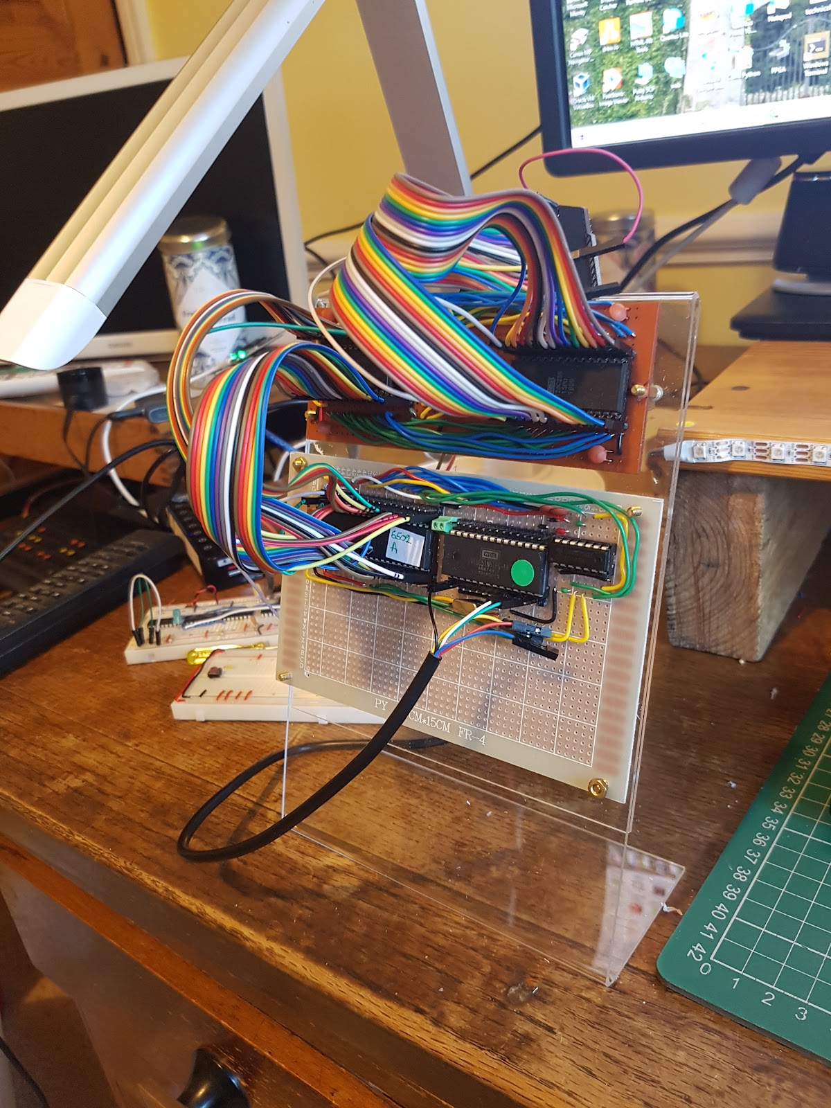
For the new board I chose an alternative strip board which provided me with 4 connection holes available on each side of the 6502 / ACIA chips. This makes CPU/ACIA connections much easier to specify.

The only downside is that I dont have +5V and GND rails provided for me so I have to "daisy chain" power connections. I underestimated the work involved with these and had to amend the design during soldering. In future I should allocate some spare tracks for power wires. Other than this problem the soldering is easier than the memory board as a lot of address wires are not required on the board. Off board connections are provided from the CPU to the memory board. There is also a spare row so that I can add a lower row of chips in the spare space at the bottom of the board and connect them to the CPU.
Once the board was soldered I could check the quality as usual by testing sdjacent shorts and circuit testing each board connection to make sure there was conductivity. Annoyingly there was one short which I missed and I later had to take everything apart to check it again later.


With soldering finished I could connect the new processor board to the memory board using dupont ribbon cables and test functionality using the same Arduino Mega sketches which I used to develop the breadboard version. Having a structured set of tests makes the process a lot easier. As mentioned above there was a shorted connection which meant the read-write pin was always in write-mode stopping the CPU from running. Once this was corrected and I had a working board I could attach my boards to their perspex backing board, hopefully making this a more permanent board.